Experimentally Synthesized 2D Materials at Rice University
Molybdenum
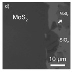
disulfide (MoS2)
Y. Zhan et al. “Large-Area
Vapor-Phase Growth and Characterization of MoS2 Atomic Layers on a SiO2
Substrate”, Small, 2012,
8, No. 7, 966–971
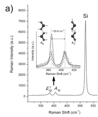
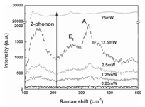
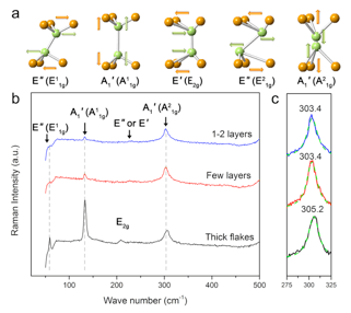
Two prominent Raman modes - symmetric in-plane E12g
and out-of-plane A1g vibrations.
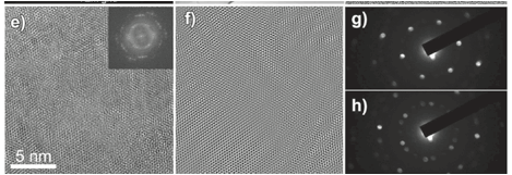
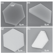
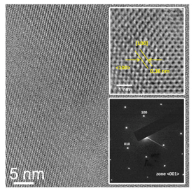
(e) shows HRTEM
image with Moiré pattern whose FFT reconstruction in (f) reveals triple layer
stack. (g) & (h) show SAED indicating hexagonal symmetry and
polycrystallinity.
Molybdenum
diselenide (MoSe2)
X. Wang et al, “Chemical
Vapor Deposition Growth of Crystalline Monolayer MoSe2”, ACS Nano, Vol.8, No. 5, pp. 5125
– 5131, 2014.
Single
crystalline monolayer flakes exhibiting large spatial extent and hexagonal
symmetry.
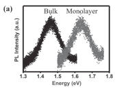
Raman active vibrations similar to MoS2 but different energies. Direct band gap ~ 1.53 eV.
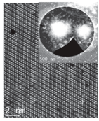
(c) shows high-res STEM image of 2H MoSe2 phase. Intensity
map shows alternating Mo & Se signals (d) shows STEM-HAADF of single and
bi-layer flakes.
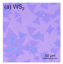
Tungsten
disulfide (WS2)
Y. Gong et al. “Tellurium-Assisted
Low-Temperature Synthesis of MoS2 andWS2 Monolayers”, ACS Nano, Vol. 9, No. 12, pp. 11658 – 11666, 2015.
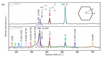
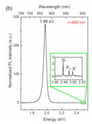
(a) shows experimental Raman spectrum of WS2 (similar to MoS2) with theoretical predictions and fitting (b) shows direct band-gap in PL spectrum at ~ 2 eV.
TEM image: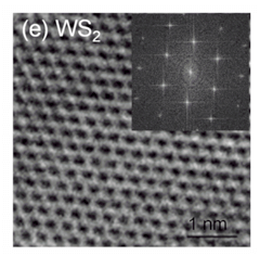
HRTEM image of WS2 monolayer
with FFT inset showing hexagonal symmetry.
Molybdenum
disulfide/ tungsten disulfide heterostructures (MoS2/ WS2)
Y. Gong et al. “Vertical
and in-plane heterostructures from WS2/MoS2 monolayers”, Nature Materials, Vol. 13, pp. 1135 – 1142, 2014.
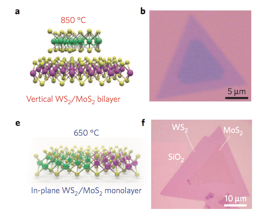
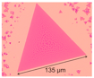
Schematics and optical images of the vertical and in-plane
monolayer heterostructures differentiable via contrast.
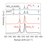
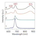
(left) Raman spectra from bottom MoS2 layer (1,2) and central MoS2/WS2 heterostructure (3.4) (right) PL spectra of (1,2) showing MoS2 direct A exciton (~1.85 eV, 680 nm) and (3.4) showing MoS2 and WS2 (~1.97 eV, 630 nm) A excitons and low energy interlayer exciton (~1.42 eV, 875 nm).
TEM image: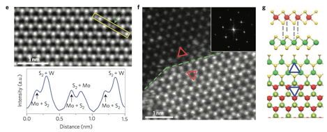
STEM image of central bilayer heterostructure showing Mo,
W, and S signals (Z-contrast).
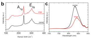
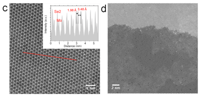
Molybdenum
diselenide/ tungsten diselenide heterostructures (MoSe2/ WSe2)
Y. Gong et al. “Two-Step
Growth of Two-Dimensional WSe2/MoSe2 Heterostructures”, Nano Letters, Vol. 15, pp. 6135 – 6141, 2015.
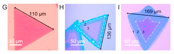
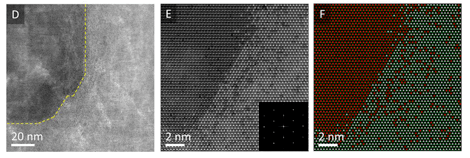
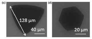
Optical images of (left) pristine MoSe2 monolayer, and Type
1 (center) and Type 2 (right) MoSe2/WSe2 bilayer heterostructures.
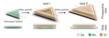
Illustrations of pristine MoSe2 (left) and the two types of
grown bilayer heterostructures.
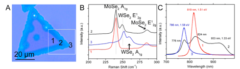
Raman spectra (center) collected from different points
(1-3) shown on left assigned to MoSe2 and WSe2
lattice vibrations. PL spectra (right) from the same regions showing individual
direct band-gaps at 1.51 eV (MoSe2), 1.58 eV (WSe2) and low energy interlayer
exciton at 1.33 eV.
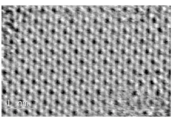
STEM image (center) of the MoSe2/ WSe2 bilayer interface
with different contrast. Atomic reconstruction (right) showing the distinct
lattices of the heterostructure.
Molybdenum
sulfide selenide (MoS2(1-x)Se2x)
Y. Gong et al. “Band Gap
Engineering and Layer-by-Layer Mapping of Selenium- Doped Molybdenum
Disulfide”, Nano Letters, Vol. 14,
pp. 442 – 449, 2014.
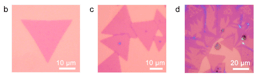
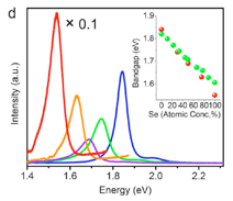
Raman spectrum (left) of an alloy composition showing characteristic MoS2 and MoSe2 lattice vibrations. PL spectra (right) as a function of atomic concentration "x" showing tunability from 1.5 eV to 1.8 eV.
TEM image: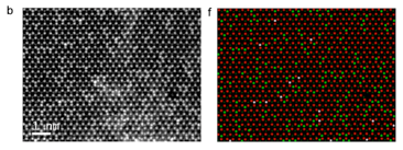
(left) STEM-ADF image of a monolayer alloy (right)
structural model showing atomic sites populated with Mo (red), S2 (dark green),
Se+S (bright green), and Se2 (white).
Rhenium
disulfide (ReS2)
K. Keyshar et al. “Chemical
Vapor Deposition of Monolayer Rhenium Disulfide (ReS2)”, Advanced Materials, Vol. 27, pp. 4640 – 4648, 2015.
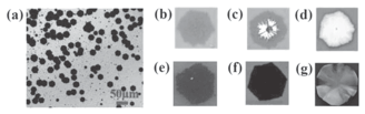
Optical images showing variety of 2D morphologies and
thicknesses of ReS2 crystals.
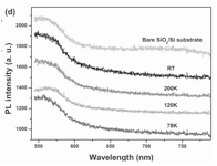
(left) Raman spectra showing wealth of active vibrational
modes due to lower symmetry of distorted 1T crystal structure (right) PL
spectra showing retention of direct band-gap but redshift with decreasing
thickness.
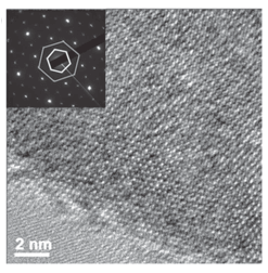
Z-contrast STEM
image showing 1T' crystal structure. Inset shows
larger area.
Tin disulfide
(SnS2)
Gonglan Ye et al.
“Synthesis of large-scale atomic-layer SnS2 through chemical vapor deposition”,
Nano Research, Vol. 5, Issue C, pp.
1 – 9, 2017.
STEM high-res image of bilayer SnS2 crystal.
Vanadium
disulfide (VS2)
J. Yuan et al. “Facile
Synthesis of Single Crystal Vanadium Disulfide Nanosheets by Chemical Vapor
Deposition for Efficient Hydrogen Evolution Reaction”, Advanced Materials, Vol. 27, pp. 5605 – 5609, 2015.
SEM images showing hexagonal VS2 layers.
(left) Raman spectra of VS2 as a function of laser power
showing prominent A1 and E2 modes (right) PL spectra as a function of
temperature showing no appreciable band-gap.
HRTEM image of VS2 sheet with SAED pattern (inset).
Indium
selenide (InSe)
S. Lei et al. “Evolution of
the Electronic Band Structure and Efficient Photo-Detection
in Atomic Layers of InSe”, ACS Nano, Vol. 8, No. 2, pp. 1263
– 1272, 2014.
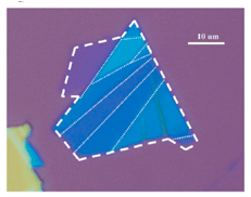
CVT-grown InSe exfoliated on top of SiO2 substrate showing
monolayer (purple) and few layer (blue) regions.
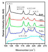
Raman spectra as a function of layer thickness showing
evolution of the mode intensities and frequencies.
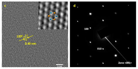
HRTEM image of monolayer InSe and corresponding SAED
pattern with hexagonal symmetry.
Gallium
selenide (GaSe)
S. Lei et al. “Synthesis
and Photoresponse of Large GaSe Atomic Layers”, Nano Letters, Vol. 13, pp. 2777 – 2781, 2013.
Optical images of Vapor phase mass transport (VMT) - grown
GaSe monolayers with various morphologies.
Raman spectra as a function of layer thickness showing
significant intensity change of A11g mode and shift in A21g
mode (right).
TEM image:
HRTEM image of [100] plane of GaSe showing lattice constant
value and SAED pattern.
Hexagonal
boron nitride (h-BN)
Z. Liu et al. “Ultrathin
high-temperature oxidation-resistant coatings of hexagonal boron nitride”, Nature Communications, Vol. 4, pp. 1
– 8, May 2013.
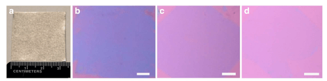
(a) Photograph of h-BN grown on Ni foil (b-d) Optical
images of bulk, few-layer, and bilayer h-BN films respectively (2 mm scale
bars).
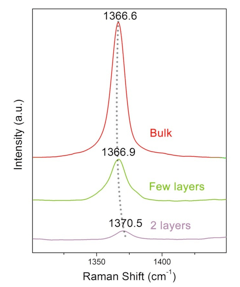
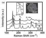
Variation in E2g Raman mode of h-BN as a
function of layer thickness.
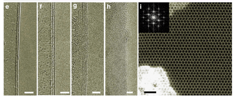
(e-h) TEM images of bi-, tri-, quad-, and multi-layered
h-BN films (i) STEM-ADF image of bilayer h-BN showing hexagonal symmetry in
SAED (inset).